
Discrete JFET vs JFET OP-Amp
Advancements in the semiconductor industry have permitted smaller feature sizes, more robust designs, and integration of components. Sensor design engineers have the option to use a simple JFET-input op-amp rather than a separate JFET in conjunction with a discrete op-amp.
Why use a discrete JFET and not a JFET-input Operational Amplifier?
There are several reasons:
- The semiconductor process used to produce op amps with integrated JFETs differs from the one used for standalone JFETs, leading to suboptimal JFET performance.
- Integrated op amps are fabricated on a monolithic die, which can lead to channel cross-coupling.
- Discrete JFETs can be selected, matched, and optimized to each application’s specific parameters.
A fundamental constraint of the integrated JFET-input op amp is due to the manufacturing process. The JFETs in the very-large-scale integration (VLSI) process are made using the same procedures and at the same time as the rest of the chip. This results in a less than optimal solution that may not be well matched to the sensor interface and cannot be individually tested or characterized. While JFET-input op amps have improved over the years, designers achieve better results by selecting the individual JFETs that are best suited for their application. It may be tempting to drop a JFET-input op amp into the circuit to make it functional, but that does not ensure that the sensor receives the best signal with the lowest noise. By matching impedances, voltage swings, and the frequency response of the JFET to the sensor, the result is a much cleaner signal sent to the digital part of the system.
While other JFET manufacturers produce monolithic dual JFETs on a single substrate, closely placed together for better temperature coefficients and matching, InterFET separates the JFETs by 0.56 millimeters; this creates adjacent dies that are matched pairs The benefit of this approach is lower crosstalk noise between the two monolithic JFETs. When both JFETs are on the same monolithic substrate, a parasitic bipolar transistor is created by the substrate which causes current to flow between the JFETs and appear as noise. InterFET matches adjacent die to stringent electrical characteristics to eliminate the parasitic transistor as a source of noise. By using adjacent die to match, the temperature coefficients and matching are still very well preserved.
Discrete JFETs can be selected, matched, and optimized to each application’s specific parameters. All designs and components have performance trade-offs. Most integrated JFET op amps are designed for lower input capacitance, with a trade-off of higher noise. If higher input capacitance is acceptable in the design, the noise can be reduced significantly with a discrete JFET front end (seen in Figure 1 below).

IF3600 matched pair front end.
e_n = 0.5\textsf{nV}/\sqrt{\textsf{Hz}} \space @ \space 1\textsf{KHz} \space @ \space G_m = 20\textsf{mS}
I_n = 10\textsf{fA}/\sqrt{\textsf{Hz}} \space @ \space 1\textsf{KHz}
LT1115
e_n = 0.9\textsf{nV}/\sqrt{\textsf{Hz}} \space @ \space 1\textsf{KHz}
I_n = 1200\textsf{fA}/\sqrt{\textsf{Hz}} \space @ \space 1\textsf{KHz}
AD743
e_n = 3.2\textsf{nV}/\sqrt{\textsf{Hz}} \space @ \space 1\textsf{KHz}
I_n = 7\textsf{fA}/\sqrt{\textsf{Hz}} \space @ \space 1\textsf{KHz}
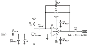
If differential input is not needed, then a single ended solution will be lower noise. Figure 2, shown below, is lower noise, and the miller capacitance is removed. This circuit is typically used to measure the noise of other devices and to measure the noise of device Q1, due to its extremely low input referred noise.
Circuit Noise less JFET Contribution
e_n = 0.1\textsf{nV}/\sqrt{\textsf{Hz}} \space @ \space 1\textsf{KHz} \space @ \space G_m = 100\textsf{mS}
IF3601 JFET
e_n = 0.35\textsf{nV}/\sqrt{\textsf{Hz}} \space @ \space 1\textsf{KHz}
IF4500 JFET
e_n = 0.85\textsf{nV}/\sqrt{\textsf{Hz}} \space @ \space 1\textsf{KHz}
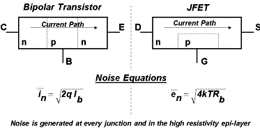
One of the differences between a JFET and a bipolar transistor is that the JFET can shut current flow to practically zero, whereas the bipolar transistor’s base current is always greater than zero; this translates to a noise injected to the signal. Another key difference of a JFET is that current flows through a single N or P type channel and does not cross a PN junction as it does with a bipolar transistor. Every time a PN junction is crossed noise is generated. This effect can be seen in Figure 3.
A JFET operates in four basic regions (see Figure 4).
- Cutoff region
- Linear region
- Saturation region
- Breakdown region
At the Gate-Source cut off voltage, the current flow through the channel is completely turned off. Since the Gate current (I_G) is near zero even when the voltage is fully cut off, the JFET makes an outstanding analog switch. For example, a 2N4117A operating at the gate-source cut off voltage will have a gate leakage current in the single digit femto-amps which translates into counting electrons as they pass. The gate leakage current is the current that escapes the gate to the source output and is a source of noise.
The output characteristics change at the Pinch-Off voltage (V_P). When the Source-Drain voltage is below the pinch off voltage region in Figure 4, the current-voltage characteristics are very linear. Allowing the JFET to function in this region enables the JFET to act as a voltage-controlled resistor. As the Source-Drain voltage increases or decreases, the Drain Current will similarly adjust in a linear fashion.
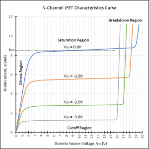
When Source-Drain voltage is above Pinch-Off voltage, in the Saturation region in Figure 4, the current is near constant over a wide range of Source-Drain voltages. This allows a JFET to funtion as a current regulator diode. For example, if the Source-Drain voltage is sufficiently greater than the Pinch-off voltage such that the noise component of the source-drain voltage does not approach the Pinch-Off voltage, then as the noise component of the source-drain voltage fluctuates, the Drain Current output will theoretically remain constant. In the real world, the Drain Current will not stay perfectly constant over a large Source-Drain voltage swing but will remain very close to constant. This is an outstanding way to supply clean current from a noisy voltage supply to a sensor or an LED.
In the breakdown region of the JFET, the device acts like a PN junction diode. Current flows and the reverse breakdown voltage level is applied.
That is seen Figure 4 as the Gate-Source voltage (V_{GS}) increases toward the gate-source cut off voltage (V_{GS(OFF)}) the amount of drain current (I_D) that is able to flow through the channel decreases for all source-drain voltages.
JFET’s are very useful when interfacing a sensor with a small output current and/or high output impedance. The JFET Gate has a very high input impedance usually specified in tera-ohms, which means that only a very small current is needed to open or close the Gate. As the Gate-Source voltage moves up or down with the sensor output, the drain current will increase or decrease. This characteristic can easily turn a sensor that is outputting a few electrons into a measurable current flow at the JFET output. This prevents the electronics from loading down the sensor and allows the JFET to act as an impedance translator from a high impedance sensor to relatively low impedance A/D.
Another interesting characteristic of JFETs is that they can be biased to achieve near zero temperature coefficient performance over a wide temperature range. As temperature increases, the mobility of the majority carriers within the channel is inhibited, about 0.8\% / \textsf{\degree C}. Any reverse biased PN junction in a JFET or bipolar transistor exhibits a barrier-potential depletion width that decreases with increased temperature, at about -2.2\textsf{mV}/\textsf{\degree C}. For the JFET, this near zero coefficient can be realized if the channel conductance decreases cause the drain current to decrease, and the gate to channel barrier-potential decreases causing the drain current to increase at the same rate to offset each other. Resulting in near zero temperature coefficient when the gate source voltage is equal to 0.63\textsf{V} less than the gate source cut off voltage. This is defined as V_{GS(OFF)}-0.63\textsf{V}. The resulting temperature compensated drift is shown in Figure 5 below.
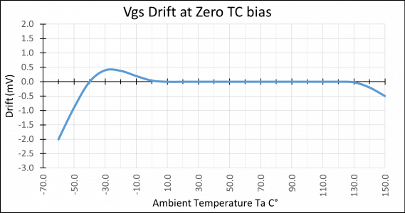
* Reference Data: Lee Evans, Siliconix Inc. Biasing FET's for Zero DC Drift
Just like the monolithic dual JFET, the JFET-input op amp has many unwanted paths to inject noise into the signal when the signal is the most vulnerable, at the sensor output. There are many examples where the design was outstanding, but the wrong JFET solution caused enough noise to overwhelm the sensor signal and resulted in poor performance at the system level. Many design engineers ignore or underestimate the importance of the analog front end and will decide that they can clean up the signal later with the DSP. All too often, however, the noise injected into the sensor signal will be enough to mask small subtle changes in the sensor output that are important to the rest of the system.