
Analog front-end solutions built on JFETs
40+ years delivering low-noise, low-power JFET solutions for the toughest analog interfaces.





About Us
For over 40 years, InterFET has been a leading manufacturer of JFETs and specialty semiconductor devices, serving audio, medical, aerospace, and industrial customers with both standard and fully custom parts.
Explore Our Offerings
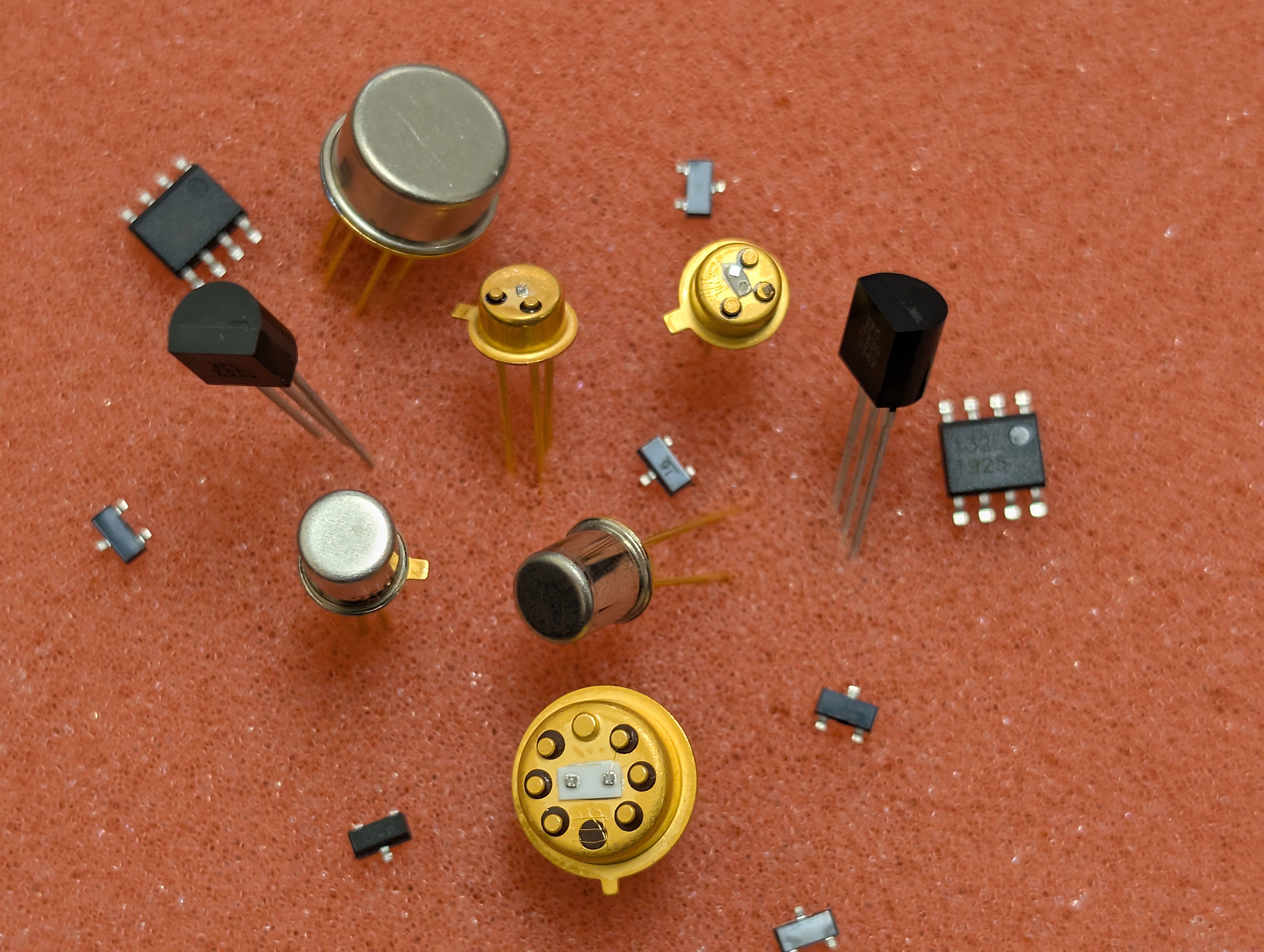
JFETs
Search and sort our complete JFET lineup by package, breakdown voltage, Idss, noise, and more.

JAN-Equivalent JFETs
Military-qualified equivalents, cross-mapped to standard parts.
Custom JFETs
Standard part doesn't meet your spec? We'll design one that does.

Buy & Support
Transactional and human-assistance routes, in one place — from placing an order to reaching an engineer.
Featured Products
Check out our most popular products
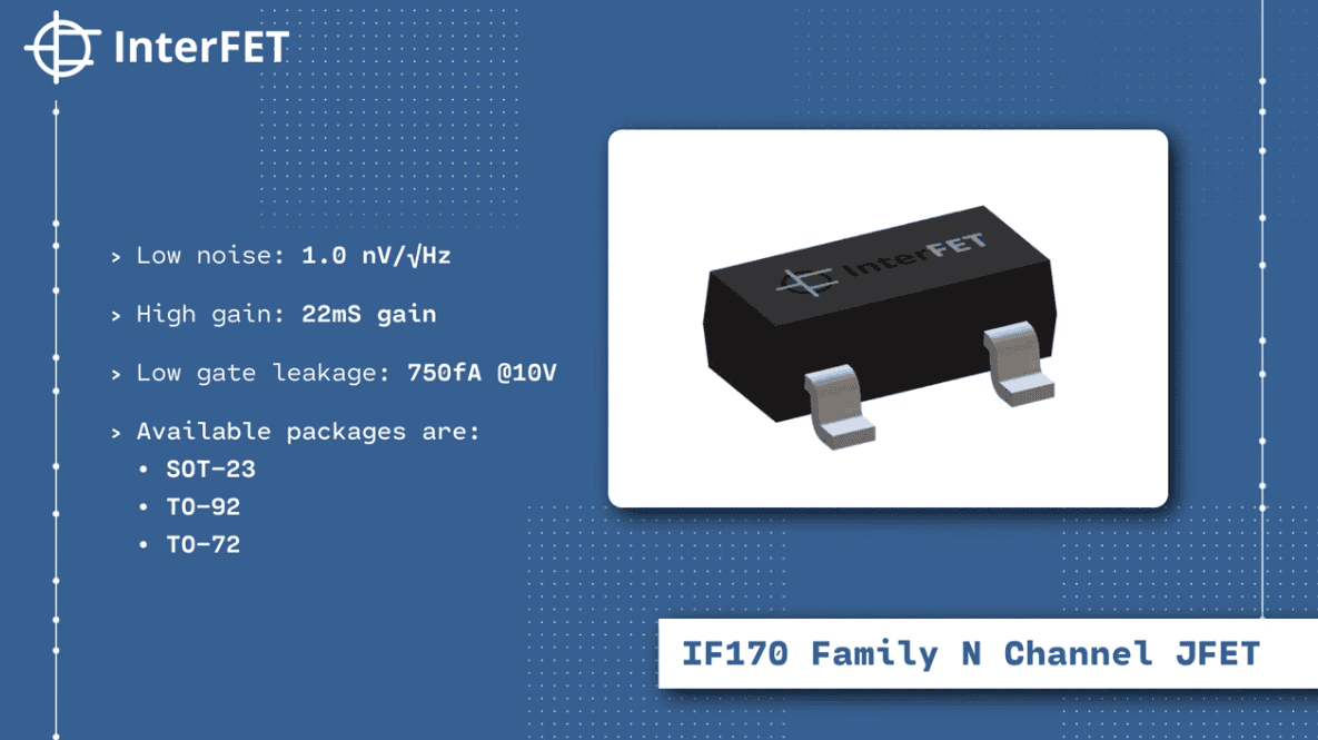
IF170 N-channel JFET
Ultra-low noise, general purpose
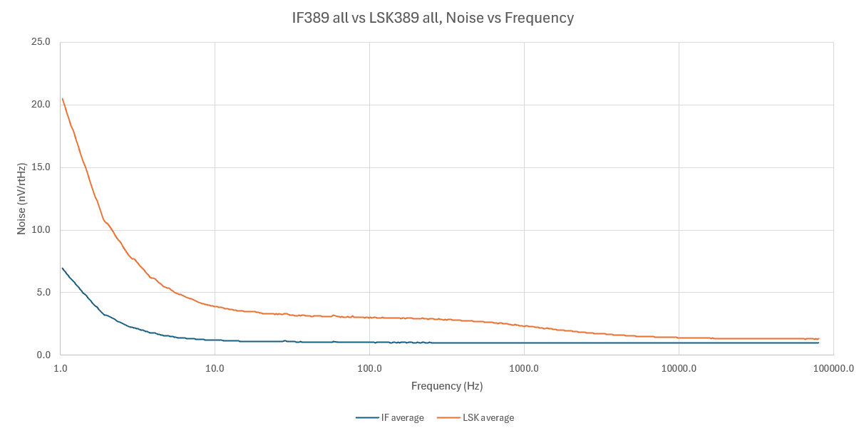
IF389 N-channel JFET
Matched-pair precision
Applications Spotlight
Explore our applications



Why Choose Us
Experience
40+ years leading the industry
Widest Range
Products to serve your applications
USA Made
Supporting Americans
Custom
Custom products are our specialty
Client Testimonials





FAQ's
The fundamental difference is how the gate controls the channel. Both devices regulate current, but they go about it in decidedly different ways.
In a MOSFET, the gate is separated from the semiconductor by a thin insulating layer. A voltage applied to the gate creates or modifies a conductive channel near the semiconductor surface.
In a JFET, the gate directly touches the channel, forming a tight seal called a PN junction.
Think of the JFET channel as a garden hose. The gate does not block the hose like a valve; instead, it uses an electric field to pinch the sides of the hose inward, narrowing the path for electricity.
A BJT (Bipolar Junction Transistor) is another common type of electronic switch, but it works on a completely different principle.
A BJT is a current controlled device; to let electricity flow through a BJT, you must continuously push a small amount of electric current into its control pin (the base). It uses two different types of electrical charges inside the material to work.
In contrast, a JFET is a voltage-controlled device; it does not need current pushed into its gate. A JFET only requires the pressure of electricity (voltage) to narrow or open the channel.
A JFET is often preferable when a circuit needs:
- Very high input impedance
- Very low input current and current noise
- Low noise with high-impedance signal sources
- Good linearity
- Low power consumption at the input
- Simple, thermally stable biasing
- The Channel is the physical “hallway” or “pipe” inside the device that electricity travels through.
- The Source is the terminal where the electrical charges enter the pipe.
- The Drain is the terminal where the electrical charges leave the pipe after traveling through the channel.
- The Gate is the control terminal that squeezes the channel to slow or stop the flow.
A JFET gate forms a PN junction with the channel. During normal operation, the gate is reverse biased relative to the channel, so only a tiny leakage current flows through that junction.
The gate still controls the channel without drawing much DC current. Changing the gate-to-source voltage changes the depletion region around the junction. For an N-channel JFET, making the gate more negative widens this region, narrows the conducting path, and reduces drain current.
This very small gate current gives a JFET high input resistance, which helps it sense weak signals without significantly loading their source. The current is not exactly zero; junction leakage generally rises with temperature, and forward biasing the gate can produce substantial current. When the gate voltage changes, the input capacitance also draws AC current.
A JFET’s high input impedance lets the device listen without interrupting. It can sense a signal while drawing almost no current from the signal source. This minimizes loading, the unwanted change in a signal caused by connecting it to a circuit.
This is particularly important for high-impedance sources such as photodiodes, pH electrodes, piezoelectric sensors, condenser microphones, and certain scientific detectors. Many of these sources whisper rather than shout; a low-impedance input can attenuate, shift, or distort their output.
A JFET’s extremely low gate current also produces very little input-current noise. This helps preserve weak signals in precision instruments and low-noise amplifiers.
High input impedance does not create gain by itself; transconductance and the surrounding circuit determines gain. Its value is that it allows the circuit to measure a delicate signal without leaning on it.
IDSS stands for Drain-to-Source Saturation Current. In simple terms, it is the maximum natural current that will flow through the JFET when the gate control is set to zero (completely wide open).
IDSS varies from device to device because small manufacturing differences affect the channel’s dimensions, doping concentration, and electrical characteristics. Manufacturers test the completed devices and sort them according to an acceptable IDSS range.
IDSS influences:
- The device’s operating or bias current
- The required source and drain resistor values
- Transconductance and gain
- Device selection and matching
In short, anyone establishing a JFET’s operating point should care about IDSS.
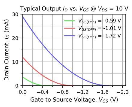
A JFET earns the description “voltage-controlled” because the gate-to-source voltage, VGS, controls the current flowing through the channel while requiring almost no steady-state gate current.
In an N-channel JFET, making the gate more negative relative to the source enlarges the depletion region and narrows the electrically conductive portion of the channel. A narrower channel allows less drain current to flow.
At VGS = 0, the conductive channel is at its widest during normal operation. As the gate becomes more negative, the channel narrows until the device approaches cutoff.
The familiar garden-hose analogy works reasonably well: squeezing the hose reduces the water flow. The squeeze comes from an electric field rather than from mechanical pressure.
Transconductance (written as gm) measures how sensitive the JFET is. It tells us how large of a change in output current we get for a tiny change in input voltage.
Transconductance is measured in siemens, or more commonly, millisiemens for a small-signal JFET. For example, a transconductance of 10 mS means that a 1 mV change in gate voltage produces approximately a 10 µA change in drain current around the selected operating point.
Higher transconductance means that a small change in gate-to-source voltage produces a larger change in drain current at the chosen operating point. In an amplifier, this can support greater gain and may help reduce input-referred voltage noise, depending on the device, its bias, and the surrounding circuit.
In a typical JFET, transconductance is highest near VGS = 0, where the drain current is near IDSS, and decreases as the device approaches cutoff. Doping, device size, and operating current all affect transconductance. Larger devices and higher operating currents can provide greater transconductance.
These two terms sound identical, but they refer to two completely different limits inside the JFET:
Cutoff (Vgs(off)) happens because of the Gate voltage. You apply so much electrical pressure (voltage) to the gate that the formerly empty depletion region grows until it completely blocks the channel. Current stops flowing entirely; the switch is off.
Pinch-off (Vp) happens because of the Drain voltage. This occurs when the drain-to-source voltage is increased enough that the depletion region constricts the channel. Once this happens, turning up the power supply voltage will not increase current flow as the flow of current levels off and becomes relatively constant.
In summary, cutoff means the channel is choked shut and current stops. Pinch-off means the channel is narrowed at the exit, causing the current to level out.
An N-channel JFET uses electrons to carry the current, runs on a positive drain supply, and is pinched off by pulling the gate negative.
A P-channel JFET is the mirror image: holes carry the current; it uses a negative drain supply and a positive gate voltage to pinch it off.
Both are depletion-mode devices that conduct fully at zero gate bias.
N-channel dominates the market because electron mobility is two to three times higher than hole mobility, giving better transconductance, lower noise, and stronger high-frequency performance, while P-channel parts exist mainly for complementary pairs.