
Why use a Discrete JFET and not just a JFET-input Op Amp?

As the semiconductor industry continues to get better processes, smaller feature sizes and more robust designs, there is a temptation by many design engineers to use a simple solution like a JFET-input op amp for their sensor input needs. In many low and mid-level applications that do not require a great deal of accuracy, this is a simple and acceptable solution, but when you only get one shot at recording an event, it is in a harsh environment, someone’s life is on the line or you want the best analog performance available, there is no substitution for a discrete JFET.
The main limitation that the JFET-input op amp or analog ASIC will encounter is caused by the way that the JFETs are manufactured. The JFETs are built with the same processes and at the same time as the rest of the circuitry. This creates less than optimal JFETs that may not be well matched and cannot be individually tested or characterized. While JFET-input op amps have improved over the years, so has the quality and specialty of discrete JFETs. The circuit designer will end up with better results by selecting the individual JFETs that are best suited for the job. Just because it is easy to drop a JFET-input op amp into the circuit and make it work, does not mean that the rest of the system is getting the best signal from the sensor with the lowest noise. By matching impedances, voltage swings, and the frequency response of the JFET to the sensor, the system will end up with a much cleaner signal to the digital part of the system.
A JFET, or Junction Field Effect Transistor, is a transistor that transports current by carriers of one polarity (majority), whereas a conventional bipolar transistor carries current of both polarities (majority and minority). The JFET is very well designed for many amplifying, switching and current regulating applications, but will never displace the bipolar transistor. The JFET, however, with its unique characteristics can make your design technically superior and often cost-effective.
The typical JFET is built on a base of silicon that will form the channel for the majority carrier flow. The channel is doped with donor impurity to create an N-type material and the channel current consists of electrons. If the channel is doped with acceptor impurity, then a P-type material is created and the majority carriers are holes. Since the electrons have greater mobility than the holes, the N-channel JFET tends to be a more efficient conductor than the P-channel JFET.
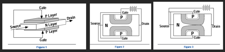
There is a gate created along the channel that has the opposite doping as the channel. By applying a voltage to the gate, a reverse-biased PN junction forms along the channel that will create a depletion region where the carriers cannot enter. As the voltage increases, the current flow will be slowly restricted as the depletion region increases. When a sufficient voltage is applied, the gate will cutoff current flow through the channel thus turning off the output as the depletion region fills the entire channel.
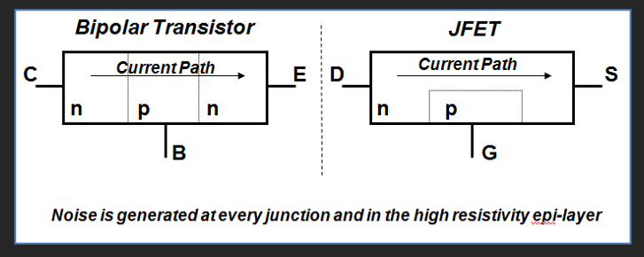
One of the differences between a JFET and bipolar transistor is that the JFET with the gate reverse-biased to turn-off channel current flow has a gate input current of practically zero, while the bipolar transistor’s base current is always greater than zero which translates to noise injected into the signal. Another reason the JFET does not inject noise into the circuit is that the current stream flows through a single N or P-type channel and does not cross a PN junction as a regular bipolar transistor would operate.
The JFET is the only type of transistor that will evenly split the load across multiple devices to increase the Voltage or Current carrying capability. By adding JFETs in series voltage capability can be increased and by adding JFETs in paralell the current carrying capability can be increased. The other characteristics like resistance or capacitance will also add or subtract in series/parallel just like descrete components would react. By contrast, bipolar transistors placed in series or parallel will have one dominant device that will carry the majority of the voltage or current until it fails.
The mechanism shown in figures 2 and 3 create a set of output curves similar to those in figure 5 for an N-type JFET. As the Voltage between the Gate and Source (VGS) increases, the output curves shift down toward the complete shut-off of the current flow. The largest output signal occurs when the Gate-Source Voltage is zero. Because of this, the JFET should be selected such that the design will allow the Gate-Source Voltage to be as close to zero as possible to provide the most dynamic output range to the system and the best performance of the JFET.
The output characteristics change at the Pinch-off Voltage (VP). When the Drain-Source Voltage (VDS) is in the Below the Pinch-off Voltage Region in figure 6, the I-V characteristics are very linear. Operating the JFET in this region will make the JFET act as a Voltage Controlled Resistor. As the Drain-Source Voltage increases and decreases, the Drain current will correspondingly change linearly.
When the Source-Drain Voltage is above the Pinch-off Voltage, in the Saturation Region in figure 6, the current is near constant over a wide range of Drain-Source Voltages. This allows the JFET to function as a Current Regulator Diode. For example, if the Drain-Source Voltage is sufficiently greater that the Pinch-off Voltage so that the noise component of the Drain-Source Voltage does not approach the Pinch-off Voltage, then as the noise component of the Drain-Source Voltage fluctuates, the Drain Current output will ideally remain constant. In the real world, the Drain Current will not stay perfectly constant over a large Drain-Source Voltage swing, but it will be very close to constant. This is an outstanding way to supply a clean current from a noisy voltage supply to a sensor or an LED.
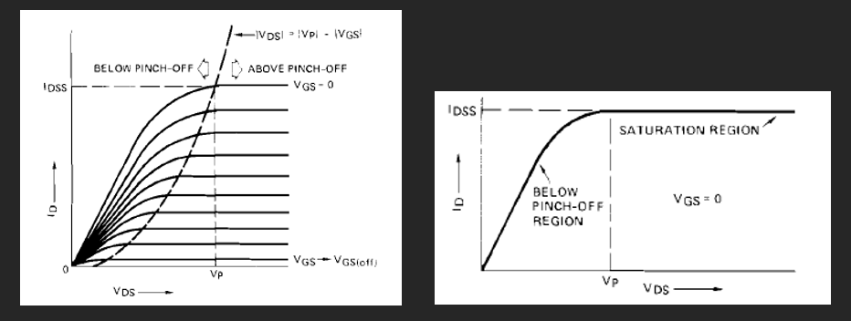
In Figure 5 you will see that as the Gate-Source Voltage (VGS) increases toward the Gate-Source Cutoff Voltage (VGS(off)), the amount of Drain Current (ID) that is able to flow through the channel decreases for all Drain-Source Voltages.
At the Gate-Source Cutoff Voltage, the current flow through the channel is completely turned off. Since the Gate Current (IG) is near zero even when the voltage is fully cutoff, the JFET makes an outstanding analog switch. For example, a 2N4117A operating at the Gate-Source Cutoff Voltage will have a Gate Leakage Current in the single digit femto-Amps which translates into counting electrons as they pass. The Gate Leakage Current is the current that escapes the Gate to the Source output and is a noise source.
One of the JFET’s characteristic is really helpful when a sensor with a small output current and/or high output impedance is used. The JFET Gate has a very high input impedance which means that only a very small current is needed to open or close the gate. As the Gate-Source Voltage moves up and down with the sensor output, the Drain Current will increase and decrease. This characteristic can easily turn a sensor that is outputting a few electrons into a measurable current flow at the JFET output. This prevents the electronics from loading down the sensor and allows the JFET to act as an impedance translator from a high impedance sensor to a relatively low impedance A/D converter.
Another interesting characteristic of JFETs is that they can be biased to achieve near zero temperature-coefficient performance over a wide temperature range. As the temperature increases, the mobility of the majority carriers within the channel is inhibited, about 0.8%/°C. Any reverse-biased PN junction, in a JFET or bipolar transistor, exhibits a barrier-potential depletion width that decreases with increased temperature, at about -2.2mV/°C. For the JFET, this near zero temperature-coefficient can be realized if the channel conductance decreases cause the drain current to decrease, and the gate-to-channel barrier potential decreases causing the drain current to increase at the same rate to offset each other. It turns out that the near zero temperature-coefficient can be achieved when the Gate-Source Voltage is equal to 0.63V less than the Gate-Source Cutoff Voltage. (VGS = VGS(off) – 0.63 V)
All of these unique characteristics of the JFET make it ideal as an input stage or impedance translator for a sensor or microphone diaphragm. At the sensor or microphone output, there is also a need for a low noise, high gain amplifier that can handle a wide frequency range without distortion or other injected noise. A good example is the InterFET IF1320 that has been in production for 30 years or if a dual device is needed, the IF1322 provides an outstanding solution for a differential signal input or precision current source.
While most of the JFET industry produces monolithic dual JFETs on a single substrate as closely placed together as possible for better temperature coefficients and matching, InterFET chooses to separate the two JFETs by just 0.022 inches and create adjacent dual die matched pairs. The reason for using two separate die that are matched is to reduce the cross talk noise between the two monolithic JFETs. With both JFETs on the same monolithic substrate, a parasitic bipolar transistor is created through the substrate which causes current to flow between the JFETs and appears as noise. InterFET matches adjacent die to stringent electrical characteristics to eliminate the parasitic transistor as a source of noise and by only using adjacent die to match, the temperature coefficients and matching are still very well preserved.
Just like the monolithic dual JFET, the JFET-input op amp has many unwanted paths to inject noise into the signal when the signal is the most vulnerable, at the sensor output. There are many examples where the design was outstanding, but the wrong JFET solution caused enough noise to overwhelm the sensor signal and cause poor performance at the system level. Too many digital designers will ignore or don’t understand that little analog front-end and will decide that they can clean up the signal later with the DSP. All too often however, the noise injected into the sensor signal in that little analog front-end will be enough to mask small, subtle changes in the sensor output that are important to the rest of the system.
Look at designing your circuit with a discrete JFET the next time your sensor or microphone needs a performance improvement. The discrete JFET will isolate your sensor from the rest of your circuitry to prevent loading of the sensor and it will increase the volume of the output available to that other circuitry without adding injected noise, cross talk or miss matching errors to that all important signal.
The world is still analog out there and until a large, clean analog signal arrives at the A/D converter, the rest of the system’s great digital processing capabilities will have nothing to work with.
About InterFET Corporation
InterFET Corporation, a privately-held company founded in 1982, is a leading manufacturer and global supplier of discrete Junction Field Effect Transistors (JFETs), custom integrated circuits and related semiconductor devices. InterFET’s corporate headquarters, operating and manufacturing facilities are located at 715 N. Glenville Drive, Suite 400, Richardson, TX in the Dallas Metroplex. More information on InterFET Corporation can be found on the website at http://interfet.com, or email TechSales@InterFET.com, or by calling 972-238-9700.