What is a JFET?
The Junction Field Effect Transistor (JFET) is a unijunction, depletion mode device that can use a voltage applied to a gate with very low leakage to vary channel current with high linearity. Featuring low noise and high radiation tolerance, JFETs are excellent transistors for different applications where precision high-gain amplification is required.
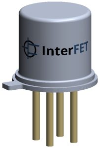
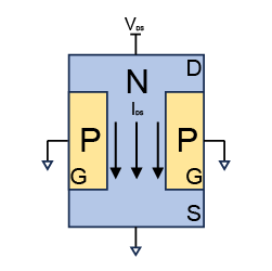
JFETs are available as N-type or P-type devices, which operate under opposite applied voltage conditions. JFETs are fabricated with the substrate of the device serving as the gate, with the channel fabricated as a layer on top of the substrate. A N-type JFET has a substrate of a semiconductor doped as P-type with N-type doping applied to the channel region, and a P-type JFET consists of a N-type substrate with a P-type channel.

JFETs operate by a similar mechanism to that of a reverse biased PN-junction, where when a diode is subjected to a positive potential difference from the N-type area to the P-type area, a depletion region will form, and no significant amount of current will be conducted between the two terminals excluding a very small leakage current.

This property is utilized in JFETs as a means of constricting the channel to reduce the current conducting from the drain to the source, where in N-type JFETs if a positive voltage is applied across the Drain to the Source (VDS≥0), and a voltage less than or equal to zero is applied across the Gate to the Source (VGS≤0), the depletion region created at the junction will be adjusting the positive Drain current (ID≥0). Conversely for a P-type JFET, if a negative voltage is applied across the Drain to the Source (VDS≤0), and a voltage greater than or equal to zero is applied across the Gate to the Source (VGS≥0), the depletion region will vary the negative Drain current (ID≤0). Figure 4 shows a comparison between a N-type JFET that is fully conducting (VGS=0) and a partially conducting one (VGS(OFF)<VGS<0).
This behavior is a key function for JFETs since the current conducted through the channel can be linearly controlled by adjusting the applied Gate to Source voltage (VGS). Furthermore, at the lower end of a device’s possible Drain to Source voltage (VDS) range, the device will be within its Ohmic region, where the Drain current can be linearly varied by both the VDS and VGS. This property alone allows JFETs to serve a variety of purposes, acting as simple amplifiers or Voltage Controlled Resistors (VCRs). Figure 5 shows the linear relation of the ID to the applied VGS, particularly at VGS values closer to zero.

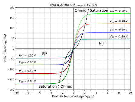
The impact of VDS and VGS on ID is a crucial characteristic to take for JFETs, which is often taken and depicted as an ID–VDS sweep. Figure 6 shows an example of this kind of sweep with a N-type JFET (NJF) and a P-type JFET (PJF) using a J109 N-type JFET and an equivalent P-type JFET. Note how in the Ohmic region, the ID is linear to the applied VDS and is linear to the applied VGS, whereas in the Saturation region, the ID is only linear to the VGS.
Two key parameters of JFETs are the Drain Current Cutoff Voltage (VGS(OFF)) and the Drain Saturation Current (IDSS). The Drain Current Cutoff Voltage is the applied gate voltage required to ideally stop all current traveling through a JFET, typically in its Saturation region. The current never completely shuts off, so VGS(OFF) is measured as the VGS required to set the drain current to below some very small value, with preferences ranging from picoamps to microamps. Figure 7 shows a simple representation of the VGS(OFF) behavior. The Drain Saturation Current is the drain current measured at a prescribed VDS in the device’s saturation region with VGS=0V.